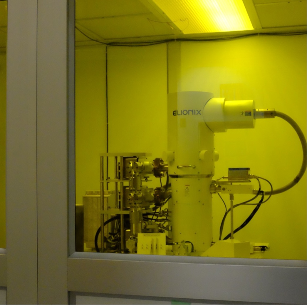
The electron-beam lithography tools facilitate writing patterns of arbitrary geometries with minimum features sizes less than 30 nanometers. Both electron-beam lithography tools share many features: field emission source, laser interferometer controlled stage capable of holding wafers op to 200 mm diameter, laser height sensing of the sample, automatic Z stage compensation, and Proximity Effect Correction (PEC) with Genisys Beamer software.
The Elionix FS-125 operates at 125 keV acceleration with a field emission source delivering 50 pA to 100 nA of beam current. The pattern generator maximum speed is 100 MHz . Field sizes available are 100, 250, and 500 microns with a pixel grid as small as 0.1nm. The stage accommodates wafers from 50 mm up to 200 mm and masks to 150 mm. A separate holder is available that holds up to 9 small pieces at one time with maximum dimension in X of 20mm, we also have a holder that allows randomly sized and shaped substrated.
The Elionix FS-125 is a user-run tool. First time e-beam lithography users should contact Mark K Mondol or Juan Ferrera with a proposed process. After meeting to discuss the process the first training session can be arranged. To become a qualified user of the FS-125 requires 4-6 hours of training over 2-3 training sessions. After completing the training users can book and use the tool on their own. Additional training may be required to learn alignment to previous features.
There are many and varied parameters that need to be considered before writing a pattern with e-beam lithography. Here is a short list:
• Substrate- material, thickness, diameter, conductivity, flatness.
• Resist type needed - positive (PMMA/ZEP/CSAR) or negative (HSQ/ma-N)*.
• Pattern transfer- how will the pattern be transferred into/onto the substrate, does it need to be transferred? How thick does the resist need to be?
• What are the smallest and largest features (or spaces) in your pattern?
• E-beam lithography produces big patterns by stitching together smaller fields, what sort of stitching errors (between fields) can you tolerate?
• What are the tolerances of your pattern; i.e. if you want 100 nm wide lines will you accept 110 nm lines or even 150 nm lines?
• Do your patterns conform to “Manhattan geometries” (i.e. orthogonal patterns) or will you require acute/obtuse angles or curves?
• Do you have precise placement objectives, either in relation to other features or for specific periodicities in your pattern, what are your tolerances?
• What is the total written area of your pattern? A grating consisting of 2500 lines that are 500 microns long about 100 nm wide and spaced 200 nm apart (i.e. 50% coverage of an area 500 x 500 microns), in PMMA, takes about 3.5 minutes to write, Using an aggressive process with 10 nA of beam current. A more conservative approach might take 14 minutes, with a 2.5 nA beam current. In other words writing 1 cm square, of 50% duty cycle or coverage, with moderate resolution takes something like 15- 60 minutes to write in PMMA; depending on your requirements for line edge roughness. Times for HSQ exposures will be significantly longer, times for ZEP will be shorter.
• What format is the pattern in, or do you still need to generate the pattern data?
• Do you want to align the pattern to some pre-existing pattern? Will you want to align subsequent e-beam patterns to previous ones? Will you want to do an optical alignment to the e-beam patterns? Do you need to align to a previously existing optically produced pattern?
• How many times might you want to write the pattern? How often will you want to change the pattern you write?
* Positive resists get developed away in exposed areas, negative resists leave resist behind in exposed areas.
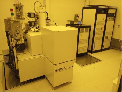
Elionix HS-50
Contact the EBL facilities manager at mondol@mit.edu with questions.
MIT Building 24 Room 041