Fab.nano is the shared fabrication facility at MIT where users carry out controlled processing of micro- and nanoscale structures. Our advanced cleanroom facilities offer capabilities ranging from lithography, etching, and deposition to diffusion, wet processing, and packaging.
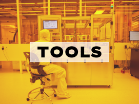
Fab.nano offers numerous tools for use by any researcher trained to use our facilities. Some individuals may come to build an entire device, while others may need to use the fab for only one portion of their project. Researchers from many different departments can work side by side, sharing the equipment and learning from each other’s processes.
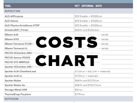
Your guide for navigating the equipment and spaces is the Fab.nano user interface. This web-based platform details the full set of toolsets across different process categories (e.g, deposition, etching, lithography); as well as specifies a tool's equipment, technical staff, base cost, and other information.
Other Charges
- Monthly access fee: $10
- Building 12 storage cubbies
- Request wafers and supplies using this form
Location
- In Building 12 (map), named the Lisa T. Su Building, the fab comprises nearly 50,000 square feet of Class 100/1,000/10,000 cleanroom, occupying the first and third floors of MIT.nano. There are also packaging and other capabilities in the fifth-floor Tecnológico de Monterrey prototyping space.
- Building 24 (map) is home to one of the tools in our electron-beam lithography (EBL) facility.
Operating hours
MIT.nano fabrication facilities are open:
Monday – Thursday: 8:00 AM – 9:00 PM
Friday: 8:00 AM – 7:00 PM
24-Hour access for the fab
24/7 access is designed for experienced users who are very familiar with the working in the fab. It is expected that a 24-hour user will not only know his/her own process, but also be familiar with the cleanrooms in general and know how to respond to all situations that might be encountered after hours. These users must also have completed the Fab.nano wet chemical processing training.
A separate training course is required for 24-hour access. More details can be found here.
24-hour status is a privilege that can be revoked at any time for safety or fab protocol violations.
MIT.nano materials
Presenting a poster at a conference or putting together a digital presentation about your research? Download MIT.nano's logos and stickers here.
MIT Lincoln Lab Microelectronics Laboratory
MIT Lincoln Laboratory’s Microelectronics Laboratory (ML) is a 200 mm wafer processing facility, equipped with commercial-class cassette-to-cassette fabrication equipment and professionally staffed 24 hours a day, five days a week. This 90 nm-class facility operates full-flow fabrication across a broad range of integrated circuit technologies, including FD-SOI CMOS, CCD imagers, superconducting electronics, photonics, MEMs, and microfluidics.
MIT.nano collaborates with Lincoln Laboratory to offer the ML's prototyping services to companies. Read more about this facility.
The Tecnológico de Monterrey Prototyping Space
All of the MIT.nano cleanroom spaces include tools and equipment that aid in the development of ideas, projects, and prototypes. The Tecnológico de Monterrey Prototyping Space located on the fifth floor serves as a specialized extension of the cleanroom complex located on the floors below.
This space is where MIT.nano can prototype functions and capabilities for our users. It includes a small Class 1,000 cleanroom area and multiple bays designed to be flexible foundations for capabilities that may be added or adapted over time.
Equipment in the Prototyping Space is part of both Fab.nano and Characterization.nano. All tools and instruments in this area are available to registered users who have completed the appropriate safety and training sessions. Read more about the MIT–Tecnológico de Monterrey Program in Nanoscience and Nanotechnology.