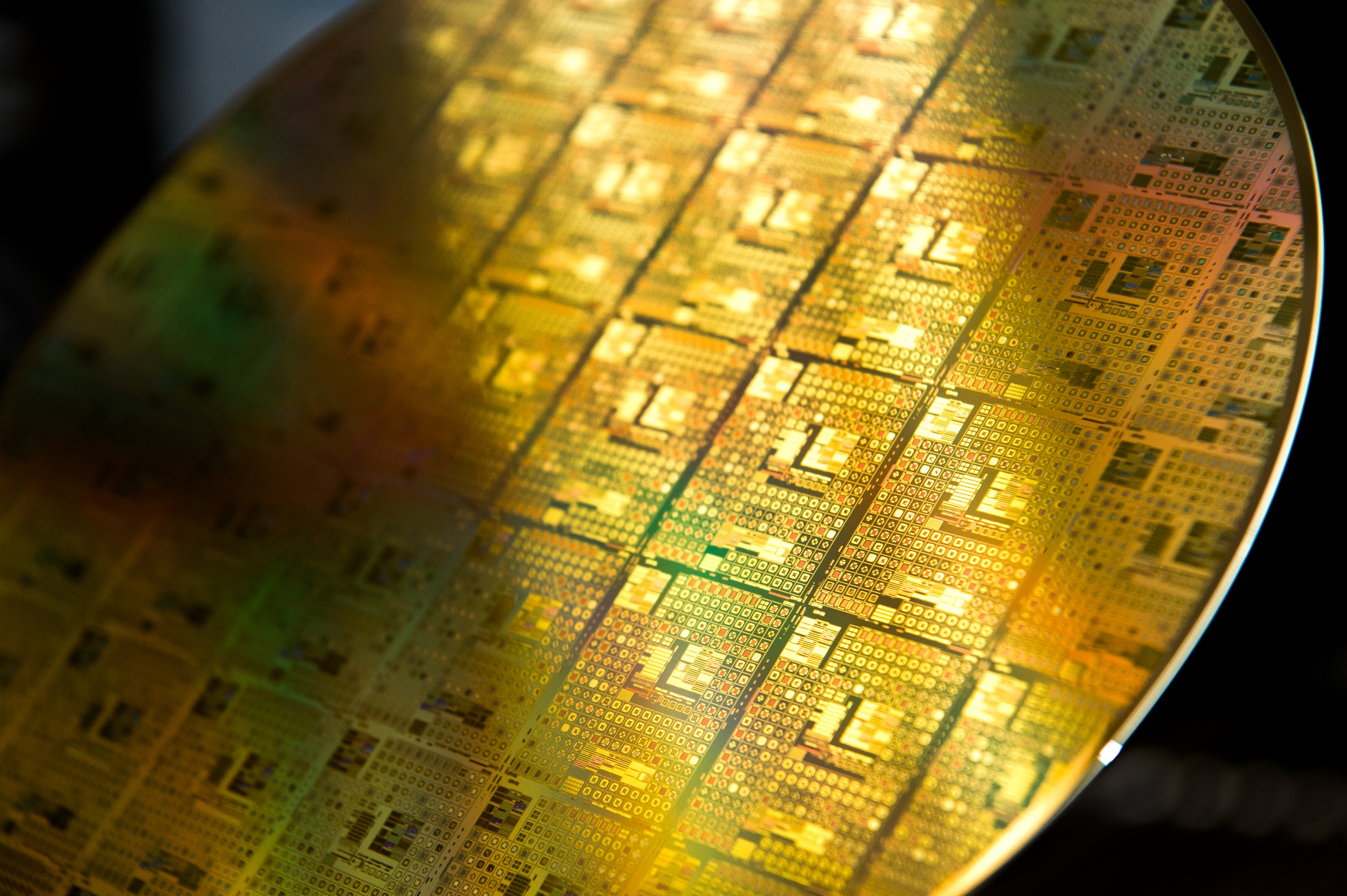
Lincoln Laboratory’s Microelectronics Laboratory (ML) is a 200 mm wafer processing facility, equipped with commercial-class cassette-to-cassette fabrication equipment and professionally staffed 24 hours a day, five days a week. This 90 nm-class facility operates full-flow fabrication across a broad range of integrated circuit technologies, including FD-SOI CMOS, CCD imagers, superconducting electronics, photonics, MEMs, and microfluidics.
MIT.nano collaborates with Lincoln Laboratory to offer the ML's prototyping services to companies. The ML is well suited for work needing large wafers, lots of small features, and process control systems to demonstrate uniformity, repeatability, process integration, or other commercial insertion risk reduction. Access fees reflect these operating expenses.
>>Microelectronics Laboratory capabilities
The Lincoln Laboratory ML provides commercial access for testing of designs, materials, and processes. Under these agreements, Lincoln Laboratory does not perform any research or development. All test data belongs to the customer. Please note that Lincoln Laboratory cannot directly compete with domestic private sector companies that also provide such testing capabilities.
If you are interested in using this facility, please complete these initial steps.