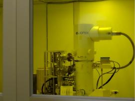
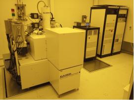
The electron-beam lithography (EBL) facility has tools in Building 12 and Building 24. These tools facilitate writing patterns of arbitrary geometries with minimum features sizes less than 30 nanometers. Both electron-beam lithography tools share many features: field emission source, laser interferometer controlled stage capable of holding wafers up to 200 mm diameter, laser height sensing of the sample, automatic Z stage compensation, and Proximity Effect Correction (PEC) with Genisys Beamer software.
Tools & Instruments
A brief introduction to e-beam lithography
As part of MIT's Independent Activities Period (IAP) 2023, Mark Mondol, assistant director for the Nano Structures Laboratory, and research scientist Juan Ferrera led a hybrid class on e-beam lithography.
This talk introduces the basics of e-beam lithography and pattern transfer, including electron energy, material interaction, limits to resolution, e-beam resists, throughput, proximity effect correction and characteristics of different e-beam lithography tools.
Links
- EBL resources: SOP's tutorials and other documents.
- EBL resists at MIT.nano
Sponsors
The MIT electron-beam lithography facility was made possible in part by generous support from the Gordon and Betty Moore Foundation, the Department of Electrical Engineering & Computer Science, Microsystems Technology Laboratories, Office of the Provost, Office of the Vice President for Research, Research Laboratory of Electronics, School of Engineering, School of Science, and faculty from across the Institute.
Contact the EBL facilities manager at mondol@mit.edu with questions.