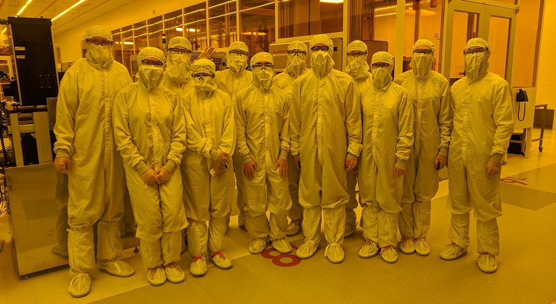
The orientation consists of a series of self-paced videos to watch, and a 30-minute check-in over zoom, where we provide an introduction, answer questions about the lab & capabilities and how to get started, and check for any missing trainings. All cleanroom and packaging space users need to complete the orientation before card access can be granted.
Users with no prior cleanroom experience also take a half-day “quick-start” class, which provides a hands-on experience in core methods (deposition, lithography, etch). Users with prior cleanroom experience will receive a waiver during the orientation check-in. If you only need to use the packaging space (and not the cleanroom), the quick-start is not needed.
Registering for the orientation, you will get a chance to describe your general fabrication needs, helping us better understand each user’s goals and expectations. The registration form also contains a checklist to help you spot any missing EHS trainings.
After registering, you will get an email with a link to the videos to watch, and the zoom link to the orientation event.