Oxford Instruments Asylum Research AFM & WITec Raman is holding a day-long, in-person workshop with morning presentations (12-0168 ) and afternoon hands-on applications topics (12-0145). Please join us for an informative day on advanced AFM and Raman capabilities at MIT.nano.
WORKSHOP SCHEDULE
9:15 AM – 9:30 AM
Welcome (Coffee and pastries sponsored by Oxford Instruments)
9:30 AM – 10:30 AM
What can I measure with an Atomic Force Microscope? Advanced AFM modes for materials characterization
Ted Limpoco, Ph.D., Senior Applications Scientist, Oxford Instruments Asylum Research
10:30 AM – 11:30 AM
Molecular visualization of 2D materials with correlative microscopy
Ute Schmidt, Applications Manager, WITec Raman
11:30 AM – 12:30 PM
Raman spectroscopy of cementitious materials
Admir Mašić, Associate Professor of Civil and Environmental Engineering, MIT
12:30 PM – 1:30 PM
Lunch sponsored by Oxford Instruments
1:30 PM – 2:00 PM
Atomic Force Microscopy of 2D materials
Ted Limpoco, Ph.D., Senior Applications Scientist, Oxford Instruments Asylum Research
2:00 PM – 5:00 PM
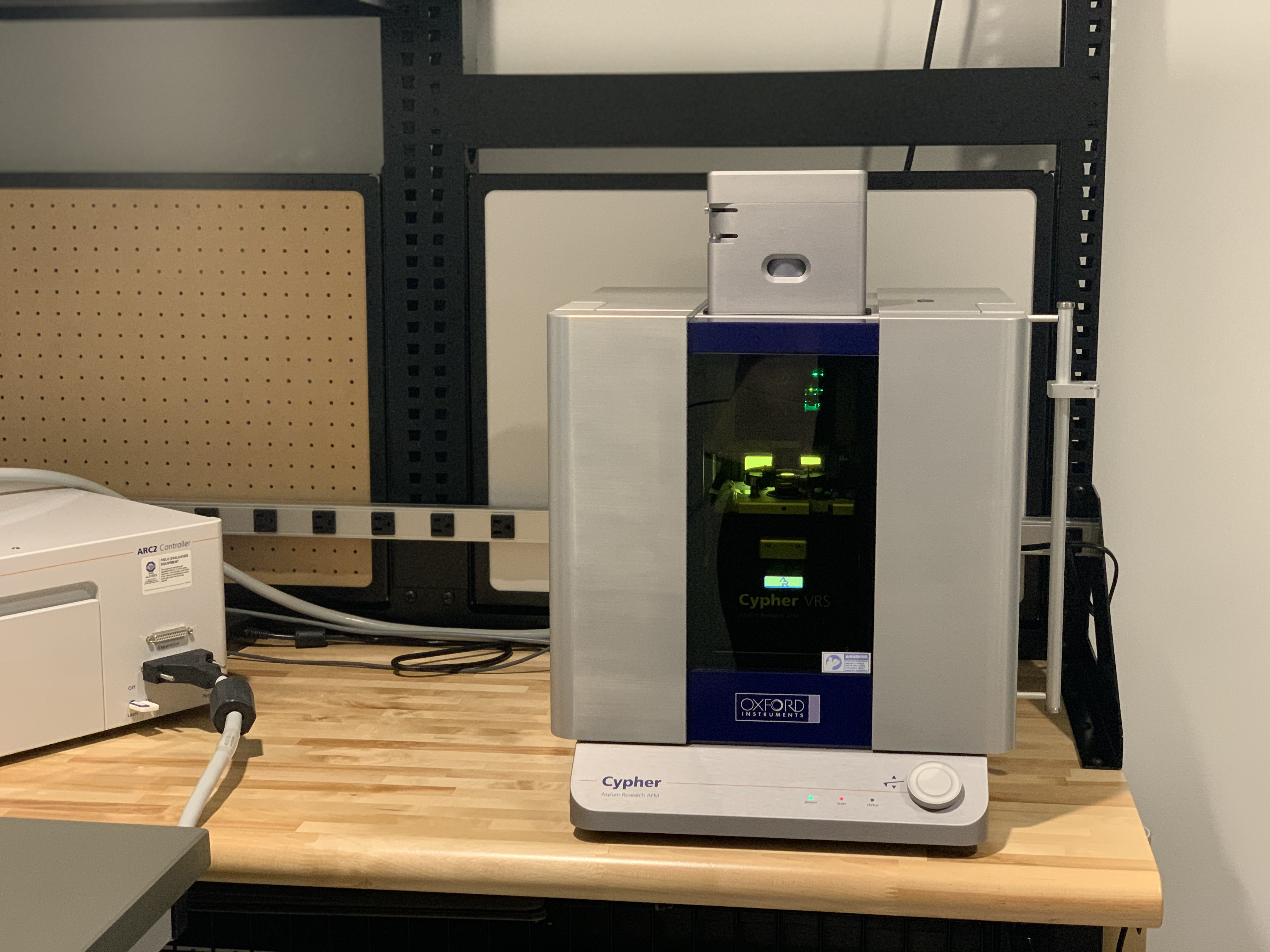
Afternoon hands-on workshop for most common applications using the Cypher VRS AFM and WITec Raman at MIT.nano (Location: 12-0195).
TALK DETAILS
LOCATION: 12-0168
TIME: 9:30 AM - 10:30 AM
TITLE: What can I measure with an Atomic Force Microscope? Advanced AFM modes for materials characterization
SPEAKER: Ted Limpoco, Ph.D., Senior Applications Scientist, Oxford Instruments Asylum Research
Atomic force microscopes (AFMs) are fundamentally visualization tools with the ability to routinely resolve topographic features of surfaces at the nanometer scale. At its highest performance, AFMs can resolve even atomic lattices and point defects. AFMs also use a mechanical probe, such that it essentially “touches” the surface, so we can obtain more information than just topography. Contact or proximity to the surface enable us to measure material properties, such as mechanical, electrical, and magnetic properties. Since the probe tip is very small, we can get very local information, mapping this on surface topography with nanometer detail. AFMs have thus become an indispensable tool in nanotechnology research.
In this presentation, we will survey advanced AFM modes that measure properties such as Young’s modulus, adhesion, and viscoelastic response (force curves, FFM, AMFM, DART-CR); current (CAFM); surface potential and work function (KPFM or SKPM); electric charge and magnetic field (EFM and MFM); capacitance, as well as dopant levels and type (SCM); and, finally, electromechanical or piezoelectric response (DART™-PFM). In the process, we will touch on advances in multi-frequency modes (DART™, AM-FM), modern methods of cantilever excitation (blueDrive™ photothermal excitation), capturing biomolecular dynamics (video-rate scanning), and imaging under environmental control.
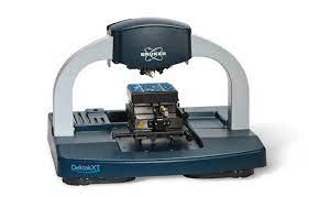
We will highlight capabilities of Asylum Research AMF tools available at MIT.nano, such as the Cypher VRS and Jupiter XR. In addition, we'll introduce Vero AFM featuring quadrature phase differential interferometric (QPDI™) technology.
These various measurement modes, combined with its ultrahigh resolution, highlight the strength and versatility of AFMs in materials characterization and nanotechnology research.
TIME: 10:30 AM - 11:30 AM
TITLE: Molecular visualization of 2D materials with correlative microscopy
SPEAKER: Ute Schmidt, Applications Manager, WITec Raman
The great success of graphene [1] kicked off the rapid growth in research on materials consisting of only one or a few layers of atoms, defined as 2D materials. In addition to graphene, other 2D materials such as transition metal dichalogenides (TMDs) have attracted increasingly attention due to their remarkable electronic and optical properties. Graphene [1,2] and TMDs [3,4] have a layered structure in common and experience significant changes in their properties with layer thickness, making them very attractive materials for electronics design [5]. For applied research and their integration with electronic circuits and sensors, the quality of the 2D materials is of great interest in terms of defects such as wrinkles, folding or lattice mismatches [6-8]. Importantly, the optical and electronic properties of 2D materials are strongly influenced by the stacking disorder [9].
The characterization tool of choice for these types of 2D materials should be non-destructive, fast, with high resolution and capable of providing comprehensive structural, optical and electronic information. This implies the combination of more than one characterization techniques to obtain a thorough understanding of their attributes for specific applications.
This talk provides insight into how optical spectroscopic imaging (Raman/Photoluminescence/SHG) in combination with AFM, contributes to an comprehensive characterization of such 2D materials.
REFERENCES
- K. S. Novoselov, A. K. Geim, S. V. Morozov, D. Jiang, Y. Zhang, S. V. Dubonos, I. V. Grigorieva and A. A. Firsov, Science 306 (2004) 666.
- Geim A. K., Grigorieva I. V., Nature 499 (2013) 419.
- M. Xu, T. Liang, M. Shi and H. Chen, Chem. Rev. 113 (2013) 3766
- J.A. Wilson & A.D. Yoffe , Advances in Physics, 18-73 (1969)193.
- Koppens F. H. L., Nueller T., Avouris P., Ferrari A.C., Vitiello M. S., Polini M., M. Nat. Nano 9 (2014) 780.
- You Y., Ni Z., Yu T., Shen Z., Appl. Phys. Letters 93 (2008) 1.
- T. Ohta, T. Becheem, J.T. Robinson, G.L. Kellogg, Phys. Rev B 85 (2012) 75415.
- S. D. Costa, J. E. Weis, O. Frank, M. Kalbac, Carbon 98 (2016) 592.
- Y. Chen, L. Meng, W. Zhao, Z. Liang, X. Wu, H. Nan, Z. Wu, S. Huang, L. Sun, J. Wang, and Z. Ni, Phys. Chem. Chem. Phys. 16 (2014) 21682.