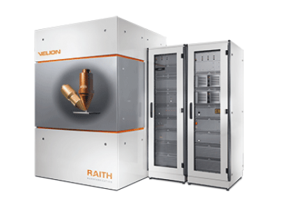
VELION is a FIB-SEM instrument dedicated to nanofabrication where Focused Ion Beam (FIB) technology has matured into state-of-the-art instrumentation for nanofabrication and rapid prototyping. VELION comprises a top down mounted nanoFIB column perpendicular to a Laser Interferometer Stage with an attached FE SEM column. The instrument offers unique capabilities and is highly optimized for fabricating high resolution, 2D and 3D nanostructures.
nanoFIB column:
- Liquid Metal Alloy Ion Sources (LMAIS) providing Wien filtered ions for Gallium-free patterning (Au, Ge, Si)
- High resolution patterning capabilities (min feature size < 15nm for Au/Si)
- Fully corrected write fields (distortion, stigmation)
- Long term current stability (up to days)
Laser Interferometer stage:
- Mechanical movement at 1nm precision
- Continuous stage modes for stitch free FIB patterning on full 4”wafer scale
- Stitching and overlay accuracy: < 50 nm (|mean|+3·sigma)
FE SEM
- Process control for rapid prototyping
Additional Capabilities:
- Automated height sensing to detect sample surface height variation for automated correction
- Pt GIS deposition
- Nanomanipulator
- Raith Nanosuite software incl. CAD (GDSII) navigation & patterning
- Plasmonic devices
- Meta materials
- Localized Ion implantation
- Nanophotonics
- Waveguides
- Fresnel lenses
- Nanofluidics
- Nanopore fabrication on waferscale
- Large area FIB hard masking
- Ga-free TEM-L prep
VELION FIB-SEM acquisition was enabled by National Science Foundation Major Research Instrumentation Program (NSF-MRI). Please make sure to acknowledge DMR-2117609 in any publication involving results originated from the use of the VELION.
Suggested language: " This work was performed in part on the Raith VELION FIB-SEM in the MIT.nano Characterization Facilities (Award: DMR-2117609)"
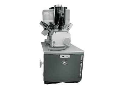
FEI Helios Nanolab 600 Dual Beam System
Juan Fererra
12-0178
MIT.nano (basement level)
60 Vassar Street (rear)
Cambridge, MA
Anna Osherov, PhD
12-5005
MIT.nano (5th floor)
60 Vassar Street (rear)
Cambridge, MA
ASSISTED USE / TRAINING REQUEST
Prior electron microscopy imaging experience is required to become an independent user
12-0189
MIT.nano (basement level)
60 Vassar Street (rear)
Cambridge, MA