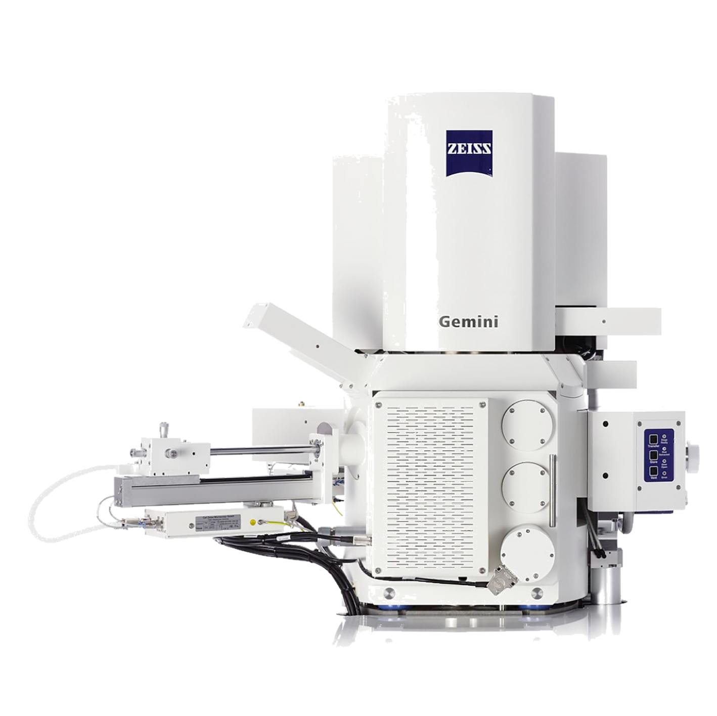
The Gemini 450 SEM, from Zeiss, is a field emission scanning electron microscope. The instrument combines ultrahigh resolution imaging with the capability to perform advanced analytics while maintaining flexibility and ease-of-use.
- Magnification: x12-2M
- Acceleration: Voltage 0.02-30kV
- Probe current: 3pA-40nA
- 5-axes motorized eucentric specimen stage (X,Y=130mm, Z=50mm, T=-4deg-70deg, R-360deg)
Detectors
- Everhart Thornley Secondary Electron Detector
- Inlens Secondary Electron Detector
- Inlens Energy Selective Backscatteres Electron Detector (EsB)
- High efficiency Variable Pressure Secondary electron Detector (VPSE)
- Angular selective Backscattered Detector
- Annular STEM Detector (aSTEM4)
- Oxford AZtec 100 EDS Detector
Imaging Modes
- High Vacuum (HV) mode – standard mode for analyzing conductive specimens.
- Variable Presurre (VP) mode – beneficial for imaging non-conductive specimens without additional specimen preparation. The partial pressure in the chamber is between 5 – 30Pa.
- Nano VP mode – enhanced VP mode with an inserted Beamsleeve aperture below the objective lens. The partial pressure in the chamber is 5 – 150Pa (350 μm Beamsleeve aperture) or 5 – 40Pa (800 μm Beamsleeve aperture).
Please make sure to acknowledge MIT.nano Characterization in any publication, presentations, and patents involving results originated from the use of the Gemini 450 SEM at MIT.nano Characterization Focus Facilities or through assistance from MIT.nano staff.
Suggested language: " This work was performed in part in the MIT.nano Characterization Facilities"
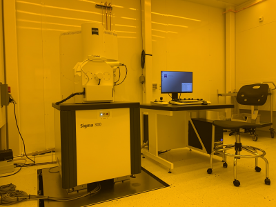
Zeiss Sigma 300 SEM
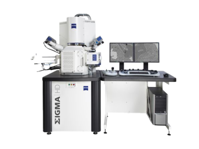
Sigma HD VP SEM
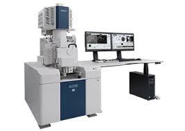
Hitachi Regulus 8100 SEM
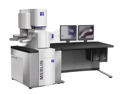
Zeiss Merlin High-resolution SEM
Only qualified users can reserve and use the instrument. The reservations are limited to 6 hr instrument time.
12-0191
MIT.nano (basement level)
60 Vassar Street (rear)
Cambridge, MA